

Laboratory Equipment & Services Information System
by Centralized Laboratory Management Office (CeLMO)
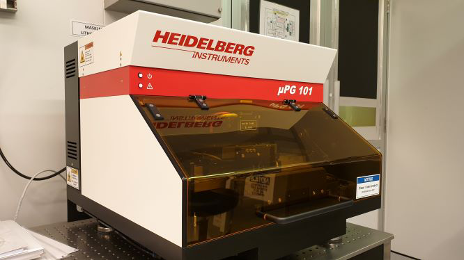
μPG 101 Maskless lithography manufactured by Heidelberg-Instruments utilizes methods that directly transfer the information onto the substrate, without utilizing an intermediate static mask, i.e. photomask that is directly replicated. In lithography process, UV radiation will be used to transfer an image of a time constant mask onto a photosensitive resist. SYSTEM FEATURES • Substrates size: up to 6” x 6” • Maximum thickness of substrate: 6 mm thickness • Flatness/ parallelism: ±20 μm • Structures down to 1 μm • UV diode laser source: 375 nm, 70 mW, laser class 3B • Maximum design size: 100 x 100 mm • Write focal length: 4 mm • Write Speed: 5 mm²/minute • Write Edge Roughness: 120 nm • Write CD Uniformity: 200 nm • Write Alignment Measurement Accuracy: 200 nm • Basic grayscale exposure mode • Exposure Optimization: Energy Series, Focus Series, Evaluation of Exposure Series • Real-time autofocus system (pneumatic, optional optical) • Camera system for alignment • Multiple design input formats: GDSII, DXF, CIF, Gerber, BMP • As an option, system come with LayoutEditor and SchematicEditor for pattern design. • The μPG 101 is equipped with rubber feet for coarse vibration isolation.
APPLICATION The μPG 101 Maskless Lithography is used for direct-write lithography process. Subsequently, it helps to skip the entire time-consuming and expensive photomask process. Besides that, the user can redesign CAD-drawing (again and again, if necessary) and immediately re-expose the pattern. This Maskless Lithography widely used for semiconductor fabrication process i.e. LED, PV, sensors, power devices & photomask production.
- Manufacturer
- Brand
- HEIDELBERG-INSTRUMENTS
- Model
- ΜPG 101
- Year Manufactured
- Year Procured
- 2019
- Department
- INSTITUT PENYELIDIKAN DAN TEKNOLOGI NANO OPTOELEKTRONIK (INOR)
- Location
- Blok A > Aras Bawah > Yellow Room
- Date Registered LESIS
- 08/02/2024
- Category
- Research Equipment
- Function
- Booking,
- Category
- Staff operated
- Equipment Status
- Good
Person In-Charge


